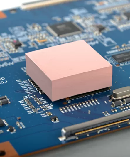
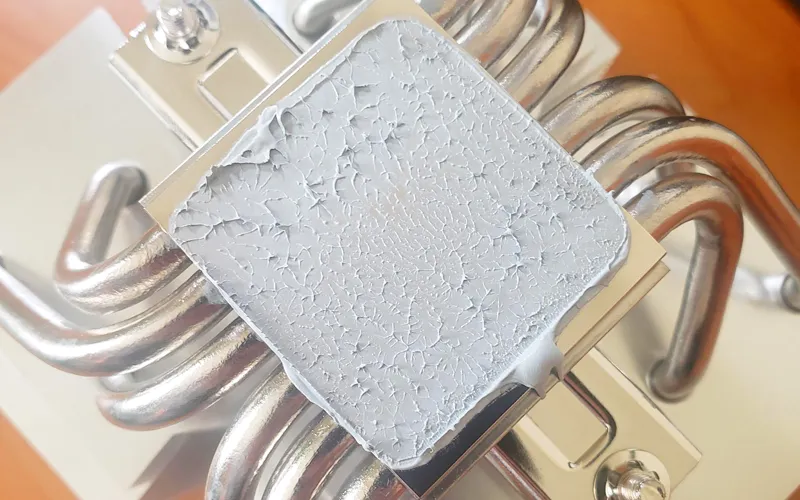
When replacing the thermal interface material on GPU VRAM, both thermal putty and thermal pads can transfer heat from memory modules to the graphics card cooler. The important difference is how they manage the physical gap.
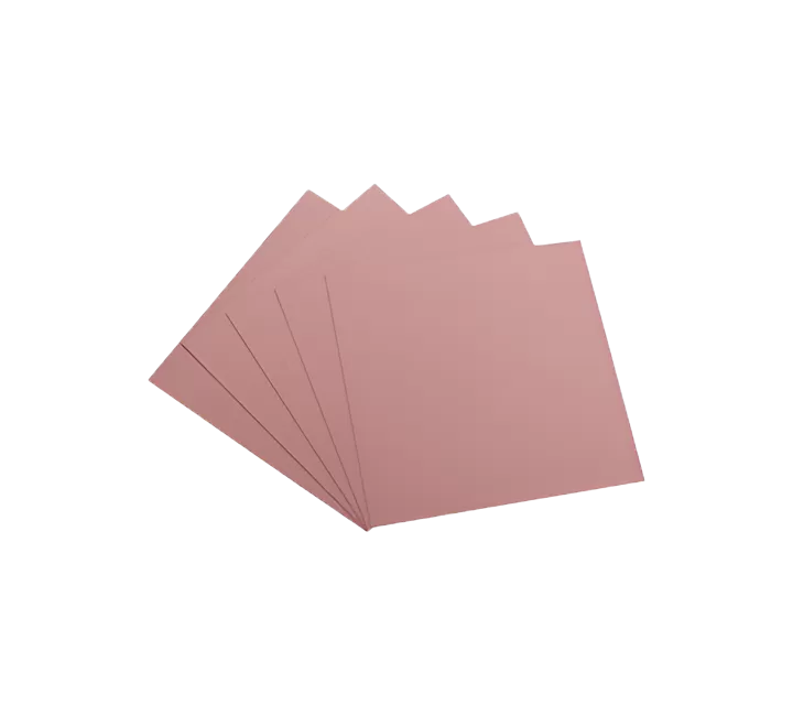
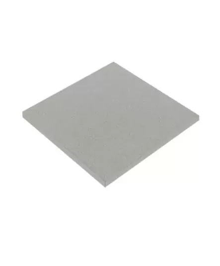
Thermal pads are preformed sheets with a controlled thickness, while thermal putty is a moldable gap-filling material that conforms to uneven component heights. For a GPU with known, consistent VRAM-to-heatsink gaps, thermal pads are usually easier to control and repeat. When the card has several component heights, uncertain gap dimensions, or difficult-to-match pad thicknesses, thermal putty can be more forgiving.
That does not mean putty is automatically better for every GPU. The best choice depends on gap height, compression pressure, cooler geometry, electrical insulation, thermal performance, rework requirements, and whether the material is being installed on one GPU or specified for mass production.
For most GPU VRAM applications:
Use thermal pads when the original pad thickness is known and the cooler requires a predictable compressed thickness.
Use thermal putty when VRAM, VRM, and nearby components have different heights or when reproducing several factory pad thicknesses is difficult.
Do not choose only by W/m·K. Contact quality, thickness, compression, voids, and cooler pressure can have a major effect on real thermal performance.
Do not use excessive material. Either an overly thick pad or too much putty can prevent the GPU die from making proper contact with its cooler.
Commercial GPU-specific putty products illustrate why this material has become popular for graphics-card servicing. Thermal Grizzly, for example, specifies its GPU gap-filling putty for height differences of approximately 0.2–3.0 mm and describes it as an electrically non-conductive alternative to conventional GPU thermal pads.
Factor | Thermal Putty | Thermal Pads |
Physical form | Moldable, paste-like or putty-like | Preformed sheet |
Gap accommodation | Excellent for varying heights | Best when gap thickness is known |
Thickness control | Determined by assembly compression | Defined by pad thickness |
Compression stress | Generally low | Depends on pad hardness and compression |
Installation | Mold or dispense onto components | Cut to size and place |
Complex VRAM/VRM layouts | Very suitable | May require multiple thicknesses |
Rework | Can be messier to remove | Usually cleaner to replace |
Mass-production repeatability | Good with controlled dispensing | Excellent with die-cut parts |
Automated assembly | Possible with suitable putty | Possible with pre-cut pads |
Risk if too much material is used | May interfere with cooler seating | Over-thick pad may prevent correct contact |
Electrical insulation | Formulation-dependent; many GPU products are insulating | Common silicone pads are electrically insulating |
AOK conductivity range | 2.0–15.0 W/(m·K) | Up to 15.0 W/(m·K) in current silicone pad range |
AOK currently offers thermal putty formulations from 2.0 to 15.0 W/(m·K), while its silicone thermal-pad portfolio includes grades ranging through 4, 5, 6, 8, 10, 12 and 15 W/(m·K).
These conductivity numbers are useful for initial screening, but they should not be treated as a direct prediction of GPU memory temperature.
The GPU core normally sits very close to the cooler cold plate and therefore uses a very thin thermal interface such as thermal grease or a phase-change material.
VRAM is different.
Memory chips, voltage-regulation components, inductors, and other devices surrounding the GPU die often sit lower than the primary cooler surface. A thermal interface therefore has to bridge a much larger physical gap between these components and the heatsink.
This is why graphics cards commonly use thermal pads over VRAM and VRM components.
The challenge is that the required height may not be identical across the entire PCB. An official GPU putty application guide from Thermal Grizzly notes that graphics cards can contain several thermal-pad thicknesses from the factory, which is one reason moldable putty is used as an alternative during GPU cooler replacement and water-block conversions.
That difference in component height is the main engineering reason thermal putty can be attractive.
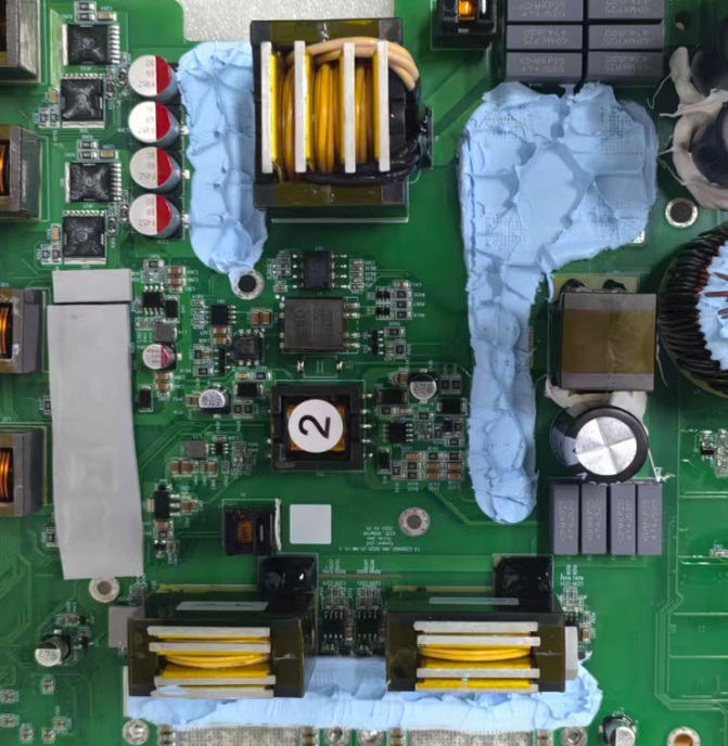
Thermal putty is particularly useful when geometry and tolerance are the main problems.
A graphics card may contain:
VRAM packages
MOSFETs
chokes
capacitors
controller ICs
other SMD components
These parts do not necessarily sit at exactly the same height.
A moldable putty can deform individually over each component, helping compensate for the differences without requiring the technician to identify several different sheet thicknesses.
One of the most common problems when servicing a used graphics card is that the factory pads have already been compressed.
Measuring a removed pad does not always tell you its original uncompressed thickness.
If the original specification is unavailable, selecting a replacement sheet can become difficult. Too thin and it may not contact the cooler; too thick and it may prevent the cooler from seating correctly on the GPU core.
Putty reduces this dependency on an exact starting thickness because excess material can deform outward when the cooler is installed.
Putty can conform around irregular VRM layouts or small components where cutting individual pads becomes inconvenient.
This is particularly useful for:
GPU repair
aftermarket cooler installation
GPU water blocks
prototypes
small production batches
non-standard PCB layouts
For projects that require repeatable dispensing rather than manual application, AOK's thermal putty application portfolio includes semi-flow and highly moldable formulations suitable for automated dispensing. AOK's broader putty range provides thermal conductivity options from 2.0 to 15.0 W/(m·K) together with electrical insulation and low-compression-stress characteristics.
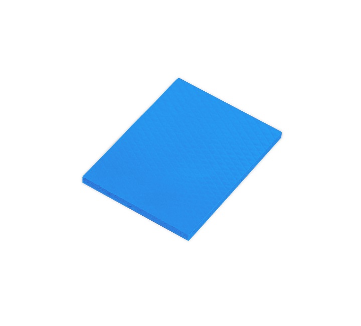
Thermal pads remain the more predictable choice when the physical dimensions of the cooling system are already well defined.
If the GPU manufacturer or cooler supplier specifies a 1.0 mm, 1.5 mm, 2.0 mm, or other exact pad thickness, a correctly selected thermal pad provides a controlled interface.
This can make assembly more repeatable.
Thermal pads are straightforward to:
cut,
position,
compress,
remove,
replace.
For field service or production environments where cleanliness and handling speed are important, this can be an advantage over putty.
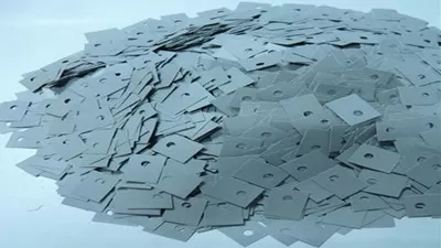
Pre-cut thermal pads can be die-cut to match VRAM and VRM geometry.
That provides advantages for OEM production:
controlled dimensions
controlled thickness
defined placement
simple operator training
easier incoming inspection
predictable material consumption
AOK, as a thermal pad manufacturer, offers thermal pads in multiple conductivity levels, thicknesses, and sizes, along with customization options for specific electronic designs. Current silicone pad grades reach up to 15 W/(m·K), while selected products are designed to provide high deformation at relatively low pressure.
For GPU servicing, choosing the wrong thermal pad thickness can create a bigger problem than choosing a slightly different thermal conductivity.
Suppose the correct interface needs approximately 1.5 mm of material.
A pad that is too thin may not fully touch the cooler.
That creates:
VRAM → pad → air gap → heatsink
Air has very poor thermal conductivity compared with a filled thermal interface material, so incomplete contact can sharply increase interface resistance.
The opposite mistake is also possible.
If the pad is too thick or too hard, the cooler may sit above its intended position. This can reduce contact pressure between the GPU die and cold plate.
Thermal Grizzly specifically warns in its high-compression GPU-pad guidance that an over-thick pad must not interfere with direct GPU-to-cooler contact. Its recommendation is essentially to use a pad that is as thin as possible but as thick as necessary.
That principle applies regardless of thermal-pad brand.
Putty eliminates the need to select an exact sheet thickness, but it does not eliminate the need to control volume.
An excessive amount of putty can:
squeeze far beyond the VRAM package
contaminate surrounding areas
increase assembly force
make future rework difficult
prevent the cooler from reaching its intended installed position
The objective is not to bury the VRAM in material.
The objective is to create enough putty volume to completely bridge the component-to-heatsink gap after the cooler reaches its correct final position.
For manual GPU servicing, the material is often shaped into portions corresponding to individual VRAM or VRM components. Commercial GPU putty suppliers specifically describe shaping small portions for VRAM and SMD surfaces rather than filling the complete PCB area indiscriminately.
There is no universal gram-per-chip specification because GPU architectures and cooler gaps vary significantly.
However, there are useful real-world reference points.
Thermal Grizzly states that approximately 30 g of its putty is generally sufficient for the front-side VRAM and voltage regulators of a large graphics card such as an RTX 4090. The same package can also be sufficient for modifying a smaller graphics card, although actual usage depends on cooler geometry and whether the backplate is also filled.
For an individual VRAM chip, the better method is therefore not to start with a fixed gram value.
Instead:
Estimate the component-to-heatsink gap.
Apply enough putty to cover the VRAM surface.
Allow sufficient material for the expected gap.
Install the cooler evenly.
Confirm that the GPU die still seats correctly.
If validating a new design, remove the cooler once and inspect the compression pattern.
For OEM applications, material volume should ultimately be controlled by a defined dispense weight or volume rather than by visual judgement alone.
A thermal pad transfers heat effectively only when it makes proper contact with both surfaces.
This means compression matters.
AOK's pad portfolio includes soft and ultra-soft silicone materials specifically designed to conform under relatively low pressure. Its TP300-H30-S, for example, is described as an ultra-soft 3.0 W/(m·K) gap-filler pad with high deformation at low pressure, while higher-conductivity ranges extend to 12 and 15 W/(m·K).
Putty behaves differently because it does not have a predefined sheet thickness. Instead, it flows or deforms until the mechanical assembly defines its final bond line.
This can help accommodate height tolerance but also means that the assembly process controls the final material thickness.
Putty is often easier where gap information is incomplete.
Pads may offer better dimensional repeatability, while dispensable putty can offer better tolerance compensation and automated material placement. If pads are the better fit for your design, thickness and compression should be selected carefully; see our guide to thermal pad for vram.
The correct answer therefore changes depending on whether you are repairing one graphics card or designing 10,000 identical assemblies.
Not necessarily.
Both products are available at high conductivity levels.
AOK currently publishes:
Thermal putty: 2.0–15.0 W/(m·K)
Silicone thermal pads: grades up to 15.0 W/(m·K)
So conductivity alone does not separate the two categories.
A simplified conduction relationship is:
Thermal resistance ≈ thickness ÷ thermal conductivity
For the same area, increasing material thickness increases thermal resistance, while higher conductivity reduces it.
This is why a 15 W/(m·K) interface that is unnecessarily thick is not automatically superior to a lower-conductivity material forming a thinner, more complete interface.
For GPU VRAM, engineers should evaluate:
actual compressed thickness
contact area
thermal conductivity
interface resistance
compression force
cooler flatness
long-term material stability
This system-level view is more useful than comparing W/m·K numbers alone.
For an individual GPU repair, you can consider putty, but there is no reason to replace correctly functioning factory pads simply because putty exists.
Keeping the original pad design may be preferable when:
the original thickness is known
the pads are still elastic
contact is complete
VRAM temperatures are normal
the cooler has been designed around those pads
Putty becomes more attractive when:
original pads are damaged
thickness information is unavailable
several pad thicknesses are required
the cooler has irregular height differences
a water block changes the original interface geometry
A GPU should also be tested after any change.
Replacing a TIM without checking the final contact condition can create a new thermal problem even when the replacement material has excellent specifications.
The same general rules apply to VRM devices.
Voltage-regulation components can generate substantial heat and often sit at heights different from VRAM.
This makes putty particularly useful where VRAM and VRM components need to contact one cooler surface despite different package heights.
However, the material must provide appropriate electrical insulation.
Many silicone thermal pads and GPU-specific putties are electrically non-conductive, but this property must be confirmed for the exact product rather than assumed for all thermal materials.
For example, AOK lists high electrical insulation as a core property of its thermal-putty portfolio and its silicone thermal pads.
This distinction is important for B2B buyers.
A material that is convenient for repairing one graphics card is not automatically the best solution for high-volume manufacturing.
Priorities often include:
tolerance compensation
ease of sourcing
uncertain original thickness
ability to cover several component heights
low assembly stress
Thermal putty can perform very well here.
Additional requirements appear:
automatic dispensing or placement
cycle time
lot-to-lot consistency
material storage
die-cut tolerances
compression-force control
electrical reliability
automation compatibility
rework yield
This is where working with experienced thermal interface material manufacturers becomes more important than simply selecting a retail TIM from a conductivity chart.
AOK has developed and manufactured thermal-management materials since 2004 and maintains ISO9001, ISO14001 and IATF16949 management-system certifications. Its thermal interface portfolio covers thermal pads, thermal putty, liquid gap fillers, thermal grease, potting compounds, phase-change materials and other electronic thermal-management solutions.
Before choosing between putty and pads for GPU VRAM, answer these questions.
VRAM and VRM heights vary.
Original pad thicknesses are unknown.
Several different pad thicknesses would otherwise be needed.
The geometry is irregular.
Low compression stress is important.
Automated dispensing is preferred in a production application.
The required thickness is known.
The gap is consistent.
Clean removal and replacement matter.
Die-cut dimensions are well defined.
High production repeatability is required.
The cooler was originally engineered around a specific pad compression.
Pads prevent the GPU die from touching the cooler.
Putty requires excessive assembly force.
Material squeezes into unwanted areas.
There are visible unfilled regions.
VRAM temperature rises after replacement.
The cooler does not sit flat after reassembly.
Yes, a suitable electrically insulating thermal putty can replace thermal pads in many GPU VRAM and VRM applications. GPU-specific putty products are explicitly designed for this purpose and can compensate for component height differences. However, cooler seating and material volume still need to be controlled.
Neither is universally better. Putty is advantageous when component heights vary or the required pad thickness is unknown. Thermal pads are advantageous when the gap is known and a repeatable compressed thickness is required.
Putty does not normally have a prescribed sheet thickness. Enough material should be applied to bridge the gap after the cooler reaches its intended installed position. Some commercial GPU putty products are specified to accommodate approximately 0.2–3.0 mm height differences, but the usable range depends on the individual formulation.
Yes. Excess material can increase assembly force or prevent the cooler from seating correctly. The most important check is that the GPU core still makes proper contact with the cold plate after the VRAM and VRM gap-filling materials are installed.
Not always. Graphics cards can use several factory pad thicknesses because VRAM, MOSFETs and other components have different heights. If different gaps exist, use the specified pad thicknesses, a sufficiently compressible pad designed for the tolerance range, or an appropriate putty.
Do not select by conductivity alone. AOK offers both thermal putties and silicone thermal pads reaching 15.0 W/(m·K), but actual performance also depends on interface thickness, compression, contact area and cooler design. A properly contacted material with appropriate conductivity may outperform a higher-rated material with poor contact.
For GPU VRAM, the difference between thermal putty and thermal pads is primarily a question of geometry, tolerance and assembly control, not simply which product has a higher thermal conductivity rating.
Thermal pads are usually the better choice when the required gap and compressed thickness are already known. Their defined dimensions make them clean, predictable and well suited to repeatable assembly.
Thermal putty is particularly valuable when GPU components have different heights, the factory pad dimensions are unavailable, or the interface needs to accommodate irregular gaps with low mechanical stress.
For individual GPU servicing, this flexibility can make putty much easier to work with. For OEM production, the decision should also consider automation, dispensing volume, die-cutting, compression, material consistency and long-term reliability.
For GPU VRAM or similar electronic gap-filling applications, AOK thermal putty can be evaluated based on the required gap, compression stress, electrical insulation, thermal conductivity and dispensing method. The specific grade should be validated against the actual cooler geometry and assembly conditions before use.
The best GPU VRAM thermal solution is therefore not simply "putty" or "pad." It is the material that creates complete contact without preventing the GPU cooler from reaching its designed position, while maintaining thermal performance, electrical insulation and long-term mechanical stability.

 +86 755 2976 5899

 English