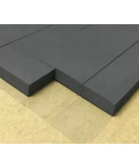
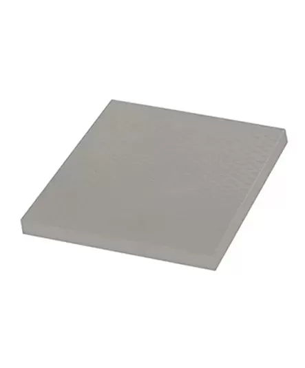
Modern electronic assemblies must manage heat while controlling electromagnetic interference (EMI). When both challenges occur in a compact space, engineers may consider an integrated thermal and electromagnetic absorber pad. A thermal pad for electronics can help transfer heat across an interface, while an absorber material can attenuate electromagnetic energy under suitable conditions. Combining these functions may simplify a design, but the correct choice depends on thermal requirements, frequency range, installation geometry, and test results.
A conventional thermal pad helps bridge a gap between a heat-generating component and a heat sink or housing. An electromagnetic absorber serves a different purpose: it is designed to reduce electromagnetic energy through absorption within a specified frequency range.An integrated absorber pad combines these functions in one material system. This can be useful when a heat-generating component is located near an electromagnetic noise source or a sensitive circuit and the design has limited space.However, absorption is not identical to shielding or grounding. A material that absorbs electromagnetic energy under one test configuration may behave differently when installed in another enclosure. Engineers should identify the interference source, frequency range, suspected coupling path, and desired improvement before selecting a material.The Federal Communications Commission's electromagnetic compatibility resources provide regulatory background. Actual product qualification still requires appropriate measurements using the relevant equipment and test setup.

The selection process should begin with the actual engineering problem, not simply a material description.For electromagnetic performance, identify the frequency band of concern, the interference path, the available mounting area, and the improvement required. For thermal performance, determine the heat load, interface gap, allowable temperature rise, mounting pressure, and expected operating temperatures.Other important considerations include:
Frequency-dependent absorption: Request data relevant to the frequencies being investigated.
Thermal conductivity and resistance: Review the measurement conditions and the proposed installed thickness.
Mechanical properties: Confirm hardness, compressibility, dimensions, and tolerance requirements.
Electrical behavior: Establish whether electrical insulation or a particular grounding arrangement is necessary.
Environmental performance: Consider temperature cycling, vibration, aging, and compatibility with adjacent materials.
Assembly constraints: Evaluate placement, available space, fastening, and repeatability.
These requirements should be recorded before comparing candidate materials. A general claim about electromagnetic absorption does not establish performance across all frequencies, just as thermal conductivity alone does not guarantee low thermal resistance in the installed assembly.
An integrated material may reduce the number of layers and simplify placement. Separate materials may provide greater flexibility when thermal and electromagnetic requirements need independent optimization.The right architecture depends on the assembly, not on a universal preference for combining functions.
| Design consideration | Integrated absorber pad | Separate thermal and absorber materials |
|---|---|---|
| Layer count | May combine functions in one layer | Usually requires separate layers or locations |
| Design flexibility | One material must meet both requirements | Each material can be selected independently |
| Space and thickness | Must fit both thermal and EMI constraints | Combined stack adds thickness and tolerances |
| Qualification | Requires thermal and frequency-specific testing | Requires individual and combined-stack validation |
| Suitable conditions | Both functions can be met by one material | Independent tuning is important |
An integrated solution is not automatically thinner, cheaper, or more effective. Engineers should compare the full assembly, including installation effort, tolerance stack-up, and performance under actual operating conditions.
Thermal and electromagnetic validation should begin as separate evaluations, followed by verification of their interaction in the assembled system.For thermal testing, use a representative heat source, contact pressure, interface thickness, and housing. Record temperatures at repeatable locations and document ambient conditions.For electromagnetic testing, define the frequency sweep, measurement equipment, probe or antenna position, cable routing, enclosure configuration, and baseline condition. Compare measurements with and without the absorber while keeping other variables consistent.Environmental testing may also be necessary. Material movement, compression changes, or loss of contact can affect thermal performance and potentially change electromagnetic behavior. For regulated electronic products, follow the applicable compliance plan and verify the final assembly.
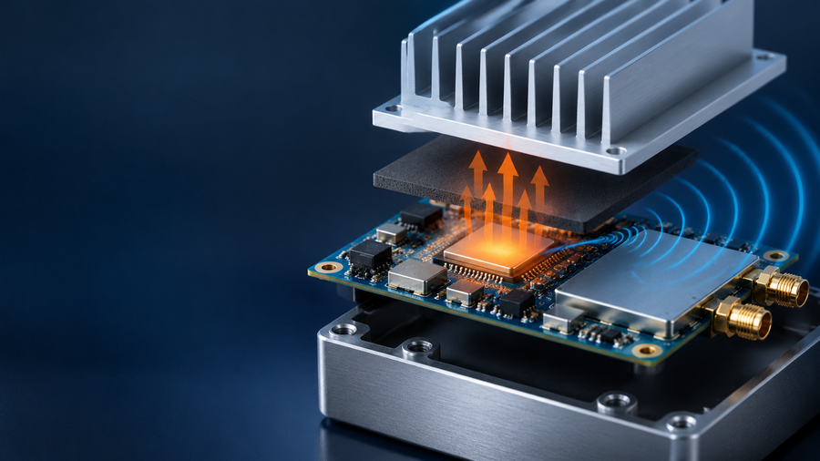
AOK Technologies offers a Thermal Electro-Magnetic Absorber Pad product range for engineering teams evaluating combined thermal-management and electromagnetic-absorption requirements.Potential candidates should be assessed against the project's frequency range, heat load, available gap, contact pressure, and installation geometry. Before choosing a model, request the latest technical data sheet and confirm the relevant thermal properties, frequency-dependent absorption data, and recommended test conditions.The AOK Technologies product catalogue provides a broader view of the company's thermal-interface material categories.For an effective technical inquiry, include the suspected interference frequency, target attenuation, component power, interface dimensions, available footprint, operating environment, and applicable test requirements. This gives the supplier a clear basis for discussing candidate materials without relying on general performance claims.
An integrated thermal-electromagnetic absorber pad may be useful when an electronic assembly must manage heat and electromagnetic interference within limited space. Selection begins with a defined frequency problem and measurable thermal requirements. Compare integrated and separate-material designs, review the relevant test data, and validate the complete assembly. AOK Technologies' absorber pad range offers candidates for evaluation, but final suitability must be established through application-specific testing.
Is an absorber pad the same as an EMI shield?
No. Absorbers attenuate electromagnetic energy, while shielding commonly limits coupling through blocking or reflection.
Will one absorber work at every frequency?
No. Performance is frequency-dependent, so request data for the relevant band.
Can an absorber replace grounding?
Do not assume so. Grounding and shielding requirements depend on the complete electrical design.
Will adding an absorber always reduce component temperature?
No. Thermal performance depends on the installed interface and its contact conditions.
What test information should a supplier provide?
Request frequency-dependent results, test methods, sample thickness, and installation conditions.
Should the final enclosure be retested after a material change?
Yes, when the change may affect thermal transfer or electromagnetic behavior.

 +86 755 2976 5899


 English