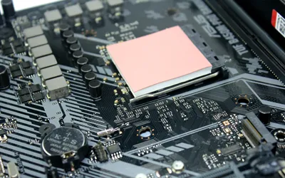
Thermal management is a key designing problem in the new generation products of semi-conductive industry, optoelectronics industry, consumption industry, automobile industry, production industry, medical industry, national defense and aviation industry. The aim of thermal management process of current electronic product is to achieve effective heat transmit from the combination part of the semi-conductor and its surroundings.

The 3 main phases of thermal transmission of electronic products:
1. Thermal transmission in the packing of the semi-conductive units
2. Thermal transmission from the units to the heat sink (the original heat sink)
3. Thermal transmission from heat sink to surroundings (the end heat sink)
The thermal transmission of the first phase is pre-decided by the device producers. The thermal transmission of the second phase and the third phase are controlledby the system thermal design engineer and the structure assembly engineer. The aim is to achieve the effective thermal transmission from the outer packing of the device to the radiator and then from the radiator to the surroundings. In order to achieve the thermal transmission goal, the designer not only needs to comprehensively understand the basic of thermal conduction, but also need to clearly master each feature of the TIM of every joint face.

TIM is used to fill the rough joint face to eliminate the void of surfaces. The nonthermal conductive air is replaced by the TIM whose thermal conductivity is much higher than the air. TIM makes the thermal resistance less than before and makes the temperature of the device packing lower. So the shelf life of the device is extended. Thermal conductivity is proportional to the area and the temperature grade. For the heat flow in steady condition, the rate is as the below fourier's law.
Thermal conductivity K is the property of the material showing the ability of heating transferring, which has no relationship with the size and shape.
Another property of the material is thermal resistance R: R=A ΔT/Q
This property is used to measure the capability to resist heat for that material with specific thickness. Combine this equation with fourier equation and rearrange it, the relation between K and R can be shown as K=d/R.

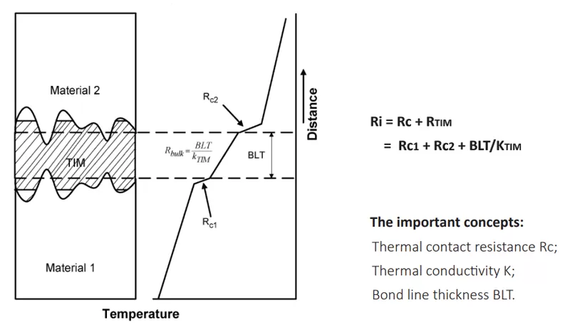
For homogeneous materials, the resistance is directly proportional to the thickness. While for heterogeneous materials, the resistance increases with the thickness increase, but not in a liner relationship. The thermal conductivity and the resistance describe the transmission after the heat into materials. Although the actual surface will never be flat or smooth, the resistance to the heat might be generated from the interface between the surface and the material. The above picture shows the irregular surface in the microscopic scale and the surface distortion in the macroscopic scale shown. The real physical contact happens at the high point and the air gap formed at depressions. The air gap resists the heat flow and forces more heat to flow from physical contact points. This kind of resistance is called surface contact resistance which exists on all the contact surfaces. The impedance of materials comprises its resistance and any other resistance on its contact surfaces.
The smoothness of the surface, the roughness of the surface, the clamping presure, the thickness of the material and the modulus of compression influence a lot on the contact resistence. Since these surface conditions might differ in different applications, the thermal impedance will change with the application's change.
The heat produced by semi-conductor should be transmitted into surroundings. So the junction temperature of components can be controlled in a safe operational condition. Generally speaking, this heat transmission process includes the transmission from the package surface to the heat sink and the heat sink can effectively transmit the heat to the surroundings. The design of the contact surface between heat sink and the package is very important so that theresistance can be minimized. It is required that the contact surface should closely contact. The surface usually makes the uneven macroscale including depressions, bulge and distorted shapes, besides it makes the microscopic-scaled roughness. When these two faces contact, the contact only happens at the high point and the air gap forms at the low point. The typical contact area might include above 90% air gap which is a resistance can not be ignored. Filling thermal interface materials into the rough, uneven contact surfacecan eliminate the air gap.
Because the conductive rate ofthe thermal interface materials is higher than the air itreplaces, the resistance and the junction temperature will be lower. In order to adapt to the changing need of the electronic packing market, AOK has developed different kinds of TlM, as below: thermal pad, electrically insulating thermal sheet, thermal conductive gap filler, silicon-free thermal pad, thermal putty, thermal grease, thermally conductive potting encapsulant.
If you would like to learn more about AOK performance thermal materials, please visit our website at www.aok-technologies.com.
